
Custom RF Transceivers
AWG Tech designs, integrates, and manufactures application-specific RF and microwave transceivers requiring specialised frequency coverage, signal conditioning, frequency conversion, amplification, and control.
Our engineering approach addresses system-level challenges involving cascaded noise figure, inter-stage impedance matching, spurious suppression, thermal management, and RF performance optimisation.
We develop custom RF transmit and receive subsystems tailored to specific electrical, mechanical, and operational requirements.
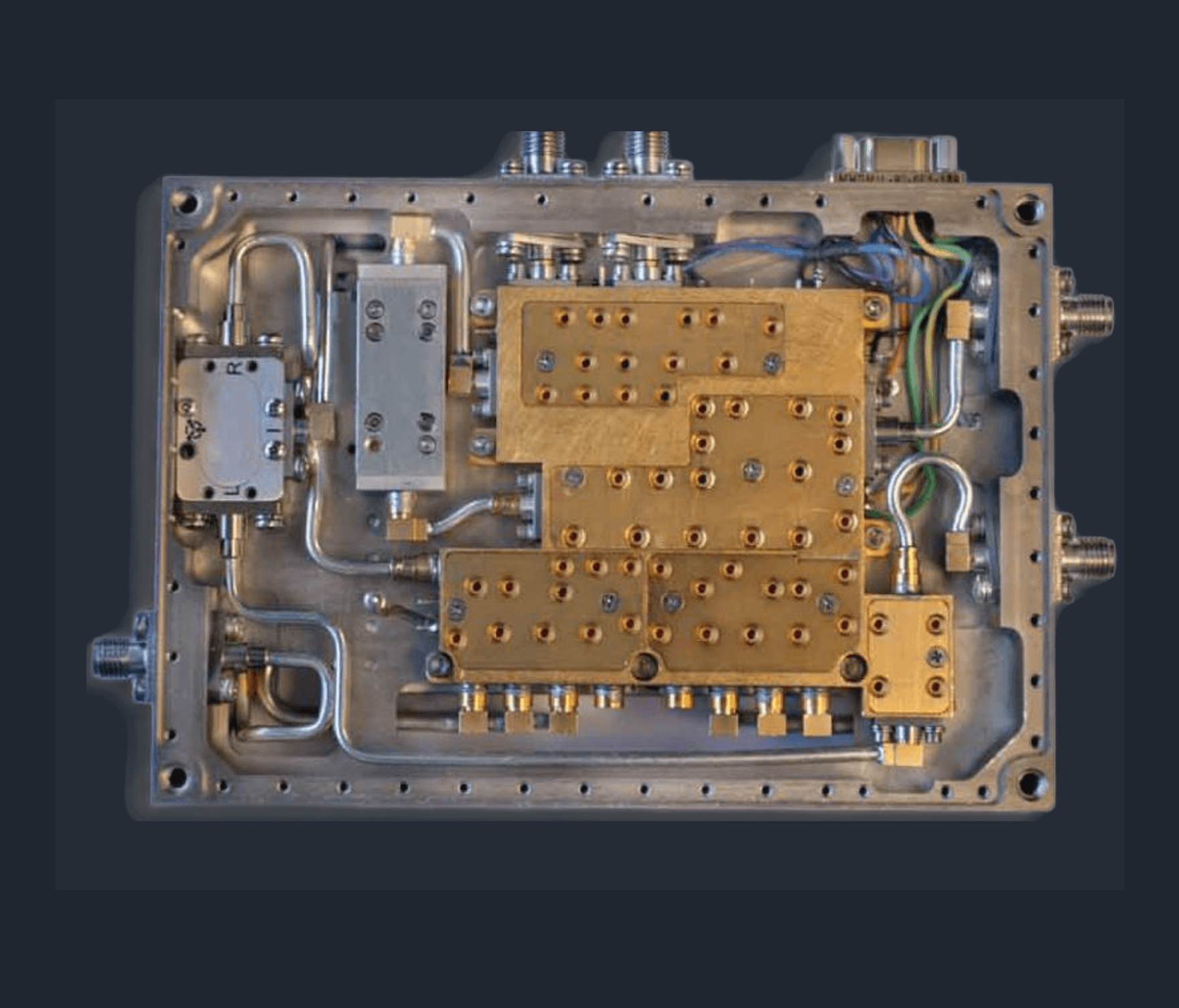
Custom RF Transceiver
Custom RF Transceiver Design — From System Architecture to Verified Hardware
A custom RF transceiver is a transmit and receive subsystem engineered to a specific frequency plan, performance budget, interface set and operating environment, rather than adapted from a catalogue part. AWG Tech designs, builds, measures and qualifies custom RF and microwave transceivers and frequency-conversion subsystems in Singapore for SATCOM, defence, radar, research and industrial programmes.
What Is a Custom RF & Microwave Transceiver?
A custom RF and microwave transceiver is an integrated transmitter and receiver subsystem engineered to operate at specified frequencies, bandwidths, signal levels, and environmental conditions.
A transceiver typically combines two functional signal paths.
The receiver converts incoming RF signals into a form suitable for demodulation, digitisation, or further processing. The transmitter converts a baseband, intermediate-frequency (IF), or other input signal into the required RF output frequency and power level.
Depending on the application, a custom transceiver may include:
-
Low-noise amplifiers (LNAs), RF preselectors, and switched filter banks.
-
RF and microwave mixers, upconverters, and downconverters.
-
Frequency synthesizers, local oscillators (LOs), and reference distribution.
-
Variable-gain amplifiers, digital step attenuators, and automatic gain control.
-
Driver amplifiers and RF power amplifiers.
-
RF switches, couplers, power dividers, and signal routing networks.
-
Digital control, telemetry, monitoring, and protection circuits.
-
Integrated power supplies, shielding, thermal management, and mechanical enclosures.
A transceiver may be implemented as a compact RF module, a multi-board subsystem, or a complete 19-inch rack-mounted assembly.
RF Transceiver Architectures and Engineering Trade-offs
Selecting the appropriate RF transceiver architecture requires careful consideration of operating frequency, instantaneous bandwidth, receiver sensitivity, dynamic range, frequency conversion requirements, power consumption, and mechanical constraints.
Superheterodyne Architectures (High Selectivity & Dynamic Range):
Superheterodyne receivers translate incoming RF signals to one or more intermediate frequencies, allowing filtering and gain distribution at different stages of the signal chain.
This architecture offers flexibility in managing image rejection, adjacent-channel selectivity, and receiver dynamic range. However, additional conversion stages introduce challenges involving local oscillator leakage, spurious responses, conversion loss, and frequency planning.
- When to choose: Mission-critical defense radar, Electronic Support Measures (ESM), and high-interference SATCOM ground terminals.
- AWG Advantage: Multi-stage conversion with distributed IF filtering to eliminate in-band half-IF and image spurs. Custom internal LO distribution with low phase noise (< -110 dBc/Hz at 10 kHz offset at X-band).
Direct Conversion (Zero-IF / Low-IF) Transceivers:
Direct-conversion receivers translate RF signals directly to baseband, potentially reducing the number of frequency conversion stages and simplifying the signal chain.
Important design considerations include DC offset, local oscillator leakage, I/Q amplitude and phase imbalance, flicker noise, and unwanted mixing products.
-
-
When to choose: Tactical UAV datalinks, software-defined payloads, and space-constrained SWaP-C environments.
-
AWG Advantage: Precision quadrature balance with automated I/Q phase/amplitude correction circuits, DC offset cancellation, and wide instantaneous bandwidth (> 500 MHz).
-
Block Up/Down Converter (BUC/LNB) Subsystems:
Block up/down converters use a single LO frequency to translate a range of RF/IF frequency to a lower/higher frequency.
-
-
When to choose: X, Ku, and Ka-band commercial and military satellite communications.
-
AWG Advantage: Integrated high-efficiency GaN/GaAs power stages with ultra-low cascaded noise receive paths, internal reference locking, and thermal compensation.
-
Custom RF Transceivers Engineering Capabilities
Developing mission-critical RF and microwave transceivers requires solving the parasitic interactions that emerge when high-gain, high-frequency active and passive stages are compressed into a dense physical envelope.
Standard datasheet ratings degrade when cascaded: inter-stage VSWR ripples elevate noise figure, radiated LO harmonics desensitize receiver front ends, and high-power GaN dissipation induces thermal phase drift.
Operating from our engineering base in Singapore, AWG Tech resolves these challenges through rigorous system-level modeling, electromagnetic co-simulation, precision microelectronic assembly, and traceable RF qualification. We engineer application-specific transceiver subsystems from DC to 40 GHz for defense, satellite communications, radar, and electronic warfare platforms.
Our engineering capabilities cover receiver front ends, transmitter chains, frequency conversion, multi-channel RF systems, signal conditioning, and integrated transceiver assemblies.
Each solution is developed around the customer's frequency plan, performance requirements, control interfaces, mechanical constraints, and operating environment.

Custom RF & Microwave Receiver Front Ends
Many front end receivers are often required to operate with low-noise and high dynamic range to maintain sensitivity in hostile, dense spectral environmnets.
Application-specific RF receiver front ends usually incorporate low-noise amplifiers, preselector filters, frequency converters, and gain-control circuits.
Engineering considerations include cascaded noise figure, receiver sensitivity, dynamic range, image rejection, intermodulation performance, and unwanted signal suppression.
Solutions can be tailored for specialised frequency coverage, multi-band operation, and demanding RF environments.
-
Cascaded Noise Figure Optimization: Strategic gain distribution achieving sub-1.5 dB noise figure in L/S/C bands and sub-2.0 dB across X/Ku bands, balancing front-end preselection losses with LNA intercept points
-
Front-End Survivability & Protection: Integration of fast-recovery PIN diode limiters capable of withstanding high-power pulsed radar leakage (up to +30 dBm CW / multi-watt peak) without compromising cascaded NF
-
Image & Out-of-Band Rejection: Multi-pole cavity, interdigital, and ceramic preselection filtering delivering >60 dBc image attenuation and deep rejection of out-of-band co-site emitters
-
Dynamic Range Management: Low-distortion automatic gain control (AGC) and digitally controlled step attenuators (0.5 dB resolution) preventing ADC saturation under strong interference.
RF Transmitters & Power Amplifier Chains
AWG Tech designs and packages solid-state transmitter chains that deliver high linearity, spectral purity, and high power-added efficiency (PAE).
RF transmitter signal chains typically incorporate frequency upconversion, driver amplifiers, power amplifiers, output filtering, and RF power monitoring.
Key engineering considerations include output power, gain flatness, linearity, harmonic suppression, spurious emissions, thermal management, and power supply stability.
Custom configurations can support continuous-wave and pulsed RF applications, subject to the required operating conditions.
Some projects which we had undertaken include:
- GaN-on-SiC & GaAs Power Topologies: Single-ended and balanced driver-and-power architectures supporting continuous-wave (CW) and high-duty pulsed radar envelopes (pulse widths down to sub-uS rise/fall times).
- Linearity & Spectral Compliance: Operating back-off and predistortion optimization ensuring third-order intermodulation (IMD3) suppression > 30 dBc and spurious/harmonic levels <-60 dBc.
- Autonomous Hardware Protection: Closed-loop automatic level control (ALC), real-time forward/reflected RF power detection, and microsecond-level automated VSWR shutdown circuits to prevent catastrophic damage from open/short antenna conditions.
RF & Microwave Frequency Converters
We design single-conversion, dual-conversion, and agile multi-octave upconverters and downconverters structured to maximize spurious-free dynamic range (SFDR)
Solutions incorporate mixers, local oscillator distribution, filtering, amplification, and signal-level control to meet application-specific frequency plans.
Particular attention is given to conversion gain, image rejection, LO leakage, phase noise, spurious responses, and inter-stage impedance matching.
Considerations for up/down converters typically are:
-
Frequency Planning & Spur Mitigation: Comprehensive (mxn) mixer harmonic budgeting to keep image frequencies, half-IF spurs, and high-order intermodulation products safely outside intermediate and baseband filters
-
Local Oscillator Synthesis & Distribution: Integrated phase-locked loops (PLL), dielectric resonator oscillators (DRO), or direct digital synthesis (DDS) locked to internal OCXO or external 10/100 MHz reference sources, achieving phase noise performance better than -110 dBc/Hz at 10 kHz offset
-
LO Leakage Suppression: Multi-cavity shielding and symmetric double-balanced mixer topologies providing > 60 dB LO-to-RF and LO-to-IF isolation to prevent in-band self-interference and spectral mask violations
Multi-Channel RF Receiver Systems
Development of multi-channel RF receiver assemblies requiring consistent amplitude, phase, and frequency response across multiple signal paths.
Engineering activities include component selection, individual channel tuning, phase and amplitude matching, channel integration, and performance verification.
Applications include coherent receiver systems, direction finding, signal monitoring, and specialised multi-channel measurement platforms.
- Tight Channel Tracking: Active amplitude and phase compensation achieving channel-to-channel phase tracking below 2.0 degrees and amplitude tracking below 0.5dB across wide operating temperature bands (-40 to +85 degrees Celsius)
- High Inter-Channel Isolation: Individual channels isolated within precision-milled multi-cavity aluminum partitions, delivering 70 dB inter-channel isolation up to 40 GHz
RF Switching & Signal Conditioning
Design and integration of RF signal-conditioning assemblies incorporating switched filter banks, digital step attenuators, RF switches, power dividers, couplers, and gain-control circuits.
These assemblies support frequency-band selection, signal routing, attenuation control, and RF level management.
Design considerations include insertion loss, isolation, switching speed, impedance matching, power handling, and repeatability across operating conditions.
-
Switched Filter Banks (SFB): Multi-throw PIN diode or fast GaAs/GaN solid-state switch matrices achieving switching speeds under 100us with high port-to-port isolation (60 dB)
-
Passive Network Integration: Monolithic integration of microstrip/stripline power dividers, directional couplers for in-situ power monitoring, and custom bandpass/notch filtering.
-
Low Insertion Loss & Group Delay Flatness: Minimized passband ripple and controlled phase linearity across octave and multi-octave bandwidths to eliminate pulse distortion in radar and EW applications.
Integrated RF Transceiver Subsystems
System-level integration of RF transmit and receive chains with frequency synthesizers, DC power supplies, digital control electronics, monitoring circuits, and mechanical enclosures.
Engineering activities cover RF architecture, subsystem integration, shielding, thermal management, wiring, interface implementation, and performance verification.
Solutions may be implemented as compact RF modules, multi-board assemblies, or rack-mounted systems tailored to customer requirements.
-
Enclosure Architectures: Precision CNC-machined Aluminum 6061-T6 dip-brazed housings with MIL-DTL-5541 clear chromate conversion or selective gold plating, engineered to meet MIL-STD-810H shock/vibration and MIL-STD-461G EMI/EMC shielding
-
Embedded Digital Monitoring & Control (M&C): Native microcontroller and CPLD integration supporting Ethernet (SCPI over TCP/IP, SNMP v3), RS-422, RS-485, SPI, and high-speed TTL blanking for real-time telemetry and remote control
-
Workmanship Standards: All surface-mount assembly, bare-die attach, gold wire/ribbon bonding, and semi-rigid coaxial harness routing executed by certified personnel in accordance with IPC-A-610 Class 3 and IPC/WHMA-A-620 Class 3
-
Form-Factor Versatility: Delivered as ultra-compact sealed modules for airborne pods/UAVs, outdoor weatherproof antenna-mounted BUC/LNB enclosures (IP67), or EIA-310 compliant 1U–4U 19-inch rack-mount chassis for earth stations and testbeds
Key Engineering Considerations in Custom RF Transceiver Architecture & Subsystem Integration
Designing high-performance custom RF transceivers requires rigorous mathematical budgeting, electromagnetic discipline, and precise component selection. The following technical breakdown transforms high-level design objectives into concrete engineering methodologies, system-level trade-offs, and verification workflows suitable for mission-critical and defense-grade platforms.
1. Receiver Noise Figure, Dynamic Range & Cascaded Gain Budgeting
Receiver sensitivity depends on the combined noise contribution and gain of the components within the receive signal chain.
- Cascaded Analysis & Friis Formulation:
Using Friis' noise equation, the cascaded noise figure can be evaluated from the gain and noise characteristics of individual stages.
Placing a low-noise high-gain amplifier close to the receiver input suppresses the noise contribution of subsequent mixers, filters, and IF amplifiers and can improve the overall noise figure.
However, excessive front-end gain directly degrades the cascaded Input Third-Order Intercept Point.
- Dynamic Range Optimization (SFDR):
Spurious-Free Dynamic Range dictates the receiver’s ability to detect weak signals in the presence of high-level in-band or out-of-band blockers.
- Engineering Implementation:
Front-end insertion losses prior to the first LNA (pre-select bandpass filters, limiters, T/R switches) add decibel-for-decibel to the overall system noise figure.
Low-loss ceramic resonator or suspended substrate stripline filters are deployed ahead of the LNA, accepting a modest selectivity trade-off to preserve sensitivity.
To prevent mixer compression, digital step attenuators (DSAs with 0.5 dB step resolution) or voltage-variable attenuators (VVAs) are integrated between gain stages to implement closed-loop Automatic Gain Control (AGC) with dynamic ranges exceeding 60 dB.
2. Frequency Planning, Mixer Intermodulatin & Spurious Suppression
Frequency conversion introduces unwanted mixing products, image frequencies, local oscillator leakage, and potential interference between conversion stages.
- Spurious Analysis & IF Selection:
High-order mixing products (e.g., 2X2 half-IF Spurs, 3*3 spurs) are calculated using non-linear mixer spur tables.
Choosing a high IF pushes the image frequency (RF +/- 2*IF) further away from the tuned RF band, easing the roll-off requirements of the image-reject pre-selection filter.
Conversely, a lower IF enables higher adjacent-channel selectivity, steeper ceramic or SAW/BAW channelization filtering, and simplified ADC digitization.
Careful frequency planning is therefore essential when selecting intermediate frequencies, local oscillator frequencies, and filtering arrangements.
Mixer spurious responses must be evaluated over the relevant input and output frequency ranges, including unwanted signals that may fall within the operating bandwidth.
AWG considers these effects during architecture development and verifies critical responses through RF measurements.
3. Signal Conditioning: RF Gain Flatness & Impedance Matching
The overall gain response of a transceiver is influenced by component gain variation, filter insertion loss, cable losses, and impedance mismatch between RF stages.
Poor inter-stage matching can produce gain ripple, frequency-dependent variations, and reduced power transfer.
These effects become particularly important in wideband RF systems and multi-stage microwave assemblies.
AWG addresses these challenges through component selection, RF matching, signal-chain optimisation, and measured performance verification.
4. Local Oscillator Phase Noise & Frequency Stability
Local oscillator performance can significantly influence receiver and transmitter spectral purity (such as EVM).
- LO Phase Noise
In receiver applications, LO phase noise can cause reciprocal mixing when strong unwanted signals are present near the desired signal. When a high-amplitude adjacent blocker mixes with the extended phase noise skirt of the LO, it folds wideband noise directly into the IF passband, degrading receiver sensitivity:
In transmitter applications, frequency synthesis and LO noise can contribute to the phase noise of the converted output signal.
- Synthesizer Topology & Spur Mitigation:
Modern frequency agile designs employ Integer-N or Fractional-N PLL synthesizers with integrated multi-core Voltage-Controlled Oscillators (VCOs). While Fractional-N allows fine frequency resolution without reducing phase detector frequency it introduces fractional boundary and sub-harmonic spurs.
Loop filters (passive 3rd- or 4th-order topologies) are carefully budgeted: wide loop bandwidths accelerate settling time and suppress inner-band VCO phase noise, while narrow loop bandwidths suppress reference clock spurs and high-frequency charge-pump noise.
Ultra-low-jitter Oven-Controlled (OCXO) or Temperature-Compensated (TCXO) crystal references provide low close-in phase noise, critical for high-order digital modulations (e.g., 256-QAM or complex radar pulse-compression waveforms).
Important considerations include reference oscillator stability, synthesizer phase noise, frequency resolution, settling time, and unwanted reference spurs.
5. Power Supply Distribution, Thermal Management & Signal Integrity
RF subsystem performance can vary with temperature, supply voltage, and operating conditions. RF and mixed-signal performance is highly sensitive to thermal gradients, parasitic feedback, and power rail ripple.
Power amplifiers, frequency synthesizers, and other active RF components may exhibit changes in gain, output power, frequency stability, and noise performance as temperature changes.
- Switching Regulators & Low-Dropout (LDO) Filtering:
Switching power supplies can also introduce conducted noise and unwanted interference into sensitive RF circuits.
For example, direct powering of sensitive VCOs, PLL charge pumps, and low-noise front-ends from Switched-Mode Power Supplies (SMPS) produces spurious sidebands via Power Supply Rejection Ratio (PSRR) limitations.
Effective RF subsystem design therefore requires attention to thermal conduction, component placement, supply filtering, grounding, shielding, and power distribution.
6. RF Isolation, Shielding & System Integration
Integrating multiple RF functions within a compact enclosure introduces challenges involving electromagnetic coupling, leakage, grounding, and unwanted signal feedback.
- Transmit-to-Receiver (T/T) isolation
Insufficient isolation between transmitter and receiver paths can degrade receiver sensitivity or, in severe cases, overload sensitive front-end components.
Insufficient duplexing or T/R switch isolation causes transmitter leakage to desensitize the receiver LNA (compression/burnout) or degrade receiver noise floor via transmitter wideband noise floor leakage.
Pin-diode switches or solid-state reflective/absorptive SPDT switches are configured in multi-throw or balanced configurations to provide > 60 dB of physical cross-isolation.
- Cavity Resonance & Mechanical Shielding
Mechanical partitioning, shielding, RF connector placement, cable routing, and grounding arrangements must be considered during system integration.
At microwave frequencies, hollow enclosure compartments behave as resonant waveguide cavities when enclosure dimensions exceed half a wavelength (λg/2).
Individual functional blocks (TX PA, RX LNA, LO Synthesis, Power Distribution) are partitioned into separate CNC-machined aluminum cavities.
Waveguide below cutoff design rules dictate all internal wall cutouts and inter-cavity channels.
Cavity resonance suppression is reinforced using tuned elastomeric microwave absorber materials (silicone matrix loaded with magnetic ferrite flakes) placed on cavity lid covers.
RF seams utilize conductive beryllium-copper (BeCu) fingerstock gaskets or fluorosilicone/silver-aluminum EMI gaskets with screw pitches maintained under λ/10 at the highest harmonic frequency.
AWG incorporates these considerations into RF module packaging and subsystem integration, followed by appropriate RF performance measurements.
CUSTOM RF ENGINEERING
Have a Custom RF Transceiver Requirement?
Discuss your frequency coverage, RF performance, interfaces and mechanical requirements with AWG Tech. We can review your application and explore a suitable engineering approach.
Email us at sales@awg.com.sg